
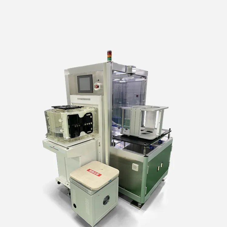
Semiconductor manufacturing requires high-speed transportation in a very clean environment. Various innovations have been made ahead of other companies to meet such demands for the wafer transport equipment used in the semiconductor processing equipment that we provide. Its high reliability and productivity are highly evaluated by customers worldwide. As a state-of-the-art industry standard equipment, we continue to evolve to meet the latest technology and diverse needs.
A device that automatically transfers silicon wafers between carriers using a transfer robot
As an additional function, it is possible to read the wafer ID laser-marked on the wafer surface and add an alignment function. In addition, regarding specifications, wafers of 200 mm and 300 mm can be handled depending on the carrier used and functions. Supports face to face transfer and back to back transfer.
Introduction of next-generation wafer Φ450mm compatible clean robot transfer equipment
Through joint research with the Gunma Industrial Technology Center, we have developed a transfer robot that can handle large silicon wafers used as next-generation semiconductor equipment. Silicon wafers are transported in a transport container to prevent dust, and are taken out, processed, and stored in the transport container for each processing step. The transport robot is a device that performs this take-out/storage.
Next-generation silicon wafers have a diameter that is 1.5 times larger, from 300mm to 450mm. For this reason, there has been a problem that the conventional transfer robot cannot perform accurate handling. This device solves this problem and enables high-speed, high-precision transfer of large silicon wafers.
This is a system that applies clean robots.
300mm wafers are transported one by one to cassettes (containers) A to B.
Compatible cassettes (containers) are FOUP, FOSB, OPEN, and PFA.
The standard transport is in units of 1 sheet, but transport in units of 5 or 25 sheets is also available.
Wafers can be safely transported collectively between cassettes.
Since wafers are lifted from the cassette for loading/unloading, contact with the cassette is minimized to prevent wear, dust generation, and damage to the wafer edge. Wafer mapping detects loading errors such as wafer misalignment and double stacking. With erroneous operation prevention sensor and emergency stop button.
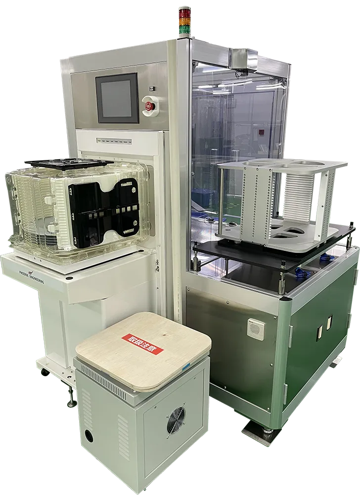
This device is φ300mm (12") quartz glass wafer stage ① ~Stage ② This is a system that automatically transfers single wafers between carriers.
The cassette used is a FOUP・FOB carrier.
Basically the carrier sets the stage to the stage.
Air cleanliness: ISO class3 (iso-14644)
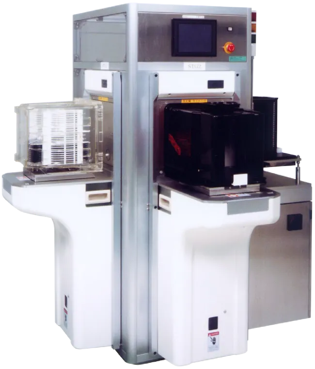
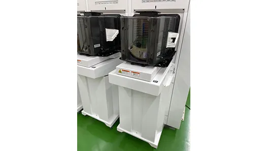
Stage 1(Loader)

Stage 2(Unloader)
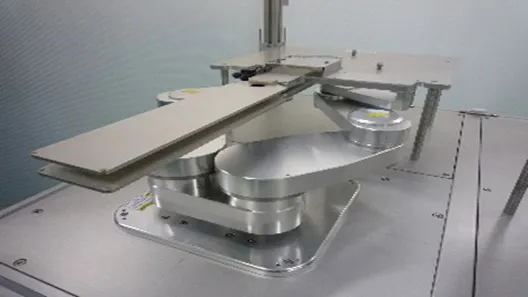
Wafer Transfer Robot